

Document Purpose: To provide the test engineer a guide in Creating a Fixture Schematic to be used on the RI 7100A tester. Though the example is for a single-site fixture the princples apply for dual-site and multi-site as well.
- Generating a DUT Functional Block Diagram.
- Generating a DIB Schematic Layout
- Generating a Fixture Schematic
To be effective in producing a working fixture the test engineer first needs to define the test needs of the DUT. A Functional Block Diagram for the purpose of assigning tester resources should then be the first step in the fixture generation process. A sample block diagram is shown below at Figure 1. The diagram should reflect the bulleted items below and be agreed upon by the test engineer and the design engineer.
- DUT Pin outs
- Voltage, Current, State, or RF requirements for each DUT pin
- External circuitry requirements for each DUT pin.
- Resource types and levels required for each pin
( ie. RF, Static Digital, Digital Programming, DC voltages, etc... ) - Handler implimentation and # of test sites.
Figure 1
Functional Block Diagram
Generating the DIB Schematic Layout:
Once the part requirements are understood then the test engineer can begin to define the Device Interface Board (DIB) using these requirements. This process helps to do the following things:
- Define the Fixture Top Assembly required.
- Define the Device Interface Board I/Os.
- Define the Fixture Carrier Board and its type (Smart vs Passive)(Single-site, Dual-site, or Multi-site).
- It should also help to define the Socket Type required for the DUT.
- Define the routing of resource lines to the DUT from the edge of the DIB.
An example of a completed DIB Schematic is shown below in Figure 2.
- Procure a copy of the standard DIB Board Template Drawing to see the actual pogo pin and RF launch positions.
- Superimpose a DUT outline drawing onto it to see how the DUT I/Os relate to these positions.
- Procure a drawing or other document that clearly shows the desired DUT pin 1 location in relation to the tester.
- Begin connecting with a pencil the DUT pins and the specific pogo pin and RF launch positions desired. Make sure that the proper DUT pin 1 location is maintained.
- Keep in mind that specific tester resources do not need to be identified at this time. Also at this time it would be advisable to begin thinking of component placement as well.
- Record the DUT pin numbers, function, and launch designation using a spreadsheet program.
- The DUT Interface Board can potentially be started at this time since the pogo pin locations and the RF launch positions are still independent of tester resources.
| Blank Template for Fixture Planning | ||
| Fixture Spreadsheet - Matrix Fixture Spreadsheet (Blank Template) |
< Major Steps >
< Major Steps > < Figure 2 > < Fixture Schematic >
Generating the Fixture Schematic (Using the Fixture Carrier Board)
After determining the DIB I/Os then the test engineer can define the Fixture Carrier Board. This step should help the engineer to make the required connections between the DIB and the Fixture Carrier Board. It should also finish with the RF connections of the Fixture Top Assembly to the Fixture Bottom Assembly. This procedure will help the engineer to:
- Define potential Fixture Modules needed to test the part.
- Define the type of carrier required (Smart vs Passive)(Single-site, Dual-site, or Multi-site).
- Provide an understanding as to what RF switching may be needed.
Steps:
- Obtain a copy of the Fixture Carrier Board Template.
- Associate with each pogo pin position on the DIB Schematic a specific test head resource as found on the Fixture Carrier Board Template. As this is done, write them down on the DIB Schematic as shown in Figure 2.
- Associate with each RF connection a position on the Fixture Top Plate. These can be found by referring to the J1-J16 numbers around the periphery of the inside cut out of the board. When doing this make sure to remember that your DIB Schematic is upside down in relation to the printed side of the Fixture Carrier Board. Also remember that the Fixture Carrier Board can only be oriented correctly in one direction to the Fixture Top Plate.
- The J numbers are associated with an RF interface at the top of the fixture. These numbers need to be associated with specific RF ports found on the Test Head itself. An RF switch needs to be added to the fixture any time a specific Test Head RF Port shows up more than once on the diagram. In the example in Figure 2, RF Test Head Port 3 shows up twice requiring a RF switch between these two points and the test head. Figure 3 represents the finished Fixture Schematic.
< Major Steps >
Fixture Schematic for Single-Site
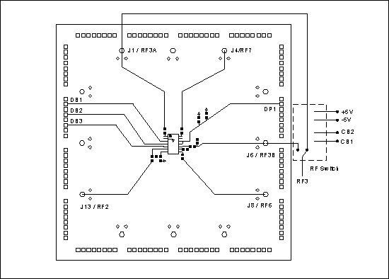
Figure 3
Fixture Schematic
Figure 3
Fixture Schematic
< Major Steps > < Fixture Schematic > < Link to Fixture Assembly Steps